Original Link: https://www.anandtech.com/show/1609
Rambus in Cell Processors and Intel's Dual Core Announcements
by Anand Lal Shimpi on February 7, 2005 3:09 PM EST- Posted in
- CPUs
Rambus in Cell
Rambus just proudly announced that their XDR memory interface would be used in the elusive Cell processor, being announced today at the International Solid State Circuits Society conference (ISSCC) in San Francisco.
There's not much surprise that Rambus was selected to be involved with the Cell project, given their previous history with Sony and the Playstation 2, as well as their ability to deliver extremely high bandwidth memory devices on very low pincounts. Sony and Toshiba also signed a licensing agreement back at the start of 2003 to work on the Cell project.
For years Rambus has been telling us that they've been working with GPU manufacturers on getting their high-bandwidth designs into future GPU architectures, and their design win with Sony may just be the key to getting XDR on PC graphics cards as well - especially since NVIDIA handled GPU design for the Playstation 3.
The other interesting part of Rambus' announcement is that they are also responsible for the Cell processor interfaces - it's connection to the outside world (or to other Cell processors). Rambus has had a serial processor bus interface in their IP repertoire for quite some time now, called FlexIO. FlexIO is being used as the processor interface standard for Cell.
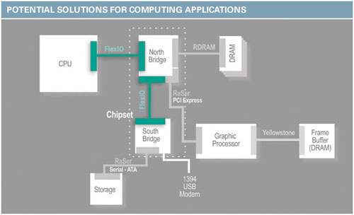
FlexIO implements two very important features - what Rambus is calling FlexPhase, and DRSL (Differential Rambus Signaling Level). Normally when traces (wires on a PCB) are laid out, they have to be arranged in such a way that all of the traces going to the same chip have equivalent lengths. As buses get wider and board designs become more complex, trace routing becomes a very serious engineering problem. Because of the need to match trace lengths, you'll often see traces wrapped around themselves or laid out in artificially long paths to make sure that the signals they carry don't arrive sooner than they should. FlexPhase is a technology that allows for on-chip data and clock alignment for signals that don't all arrive at the same time, allowing for traces that aren't matched in length on the PCB. There is an added element of latency introduced by FlexPhase as the chip must handle all clock and data adjustments that are out of phase, but the idea is that what you lose in latency do to FlexPhase, you make up for it in design simplicity, potentially allowing for higher data rates.
The next technology that FlexIO enables is DRSL with LVDS (Low Voltage Differential Signaling), which is a technology similar to what Intel uses in the Pentium 4 to reduce power consumption of their high-speed ALUs. We will actually explain the technology in greater detail later on this week in unrelated coverage, but the basic idea is as follows: normally the lower the voltage you run your interfaces at, the more difficult it becomes to detect an electrical "high" from an electrical "low." The reason being that it is quite easy to tell a 5V signal from a 0V signal, but telling a 0.9V signal from a 0V signal becomes much more difficult. DRSL instead takes the difference between two voltage lines with a very low voltage difference and uses that difference for signaling. By using low signal voltages, you can ensure that even though you may have a high speed bus, power consumption is kept to a minimum. The technology isn't quite sophisticated enough to make the transition to the mobile world, but with some additional circuitry to dynamically enable/disable interface pins it would be quite easy to apply FlexIO to mobile applications of the Cell architecture.
The culmination of these two features is that FlexIO offers up to 8.0GHz data rates based off of a 400 - 800MHz interface clock. It is worth noting that such a high input clock frequency would inherently require some pretty sophisticated technologies to implement.
Because Rambus is providing both the memory and processor I/O interfaces for Cell, it's not too surprising that 90% of the Cell's signaling pins are using Rambus interfaces. Looking at any modern day microprocessor, the biggest use of signaling pins goes to things like enabling multiprocessor support, a chipset interface and a memory interface (obviously varying based on the type of processor we're talking about) - so Rambus' statistics aren't too surprising.
There are still some unanswered questions - mainly whether or not FlexIO will be used to interface with NVIDIA's graphics core (which we're guessing it will) and whether or not XDR will be used for the GPU's local memory (which we're also guessing it will). Given the negative impression of Rambus amongst PC enthusiasts, a successful implementation in PS3 and with NVIDIA's GPU could mean a virtual second chance for Rambus in the PC market.
Intel’s Happy about Dual Core
While AMD has been touting dual core for quite some time, it’s looking like Intel will beat them to the punch - at least on the desktop. Intel had a couple of interesting announcements this morning as well.
The first thing they sent out to us was an interesting fact - that Intel has 11 multi-core projects that they’re working on for the 2005 - 2006 time period. Doing a quick number check we’re left with the following breakdown:
3 - “Smithfield” based Pentium 4 8xx series CPUs
1 - dual core Pentium 4 Extreme Edition
3 - “Yonah” based Pentium M CPUs (in 2006)
That leaves us with four unaccounted for chips - we’d expect Xeon and Itanium to fill in those blanks nicely.
Intel confirmed what we wrote about in our most recent roadmaps - the first dual core desktop CPUs will be arriving next quarter. Intel is going to be releasing two CPUs, one 90nm Extreme Edition and one 90nm Pentium 4 8xx model.
What’s interesting is that the 90nm dual core Pentium 4 Extreme Edition will feature Hyper Threading support, something that is left out of the regular Pentium 4 8xx series. A Hyper Threading enabled dual core Pentium 4 EE would mean 4 logical processors, capable of executing 4 simultaneous threads across the two physical cores. It looks like the EE chip will be launched with the new 955X chipset (Glenwood), with support for the 1066MHz FSB and DDR2-667 support. We often wondered why Intel wasn’t using the 1066MHz FSB with their Smithfield dual core processors, now we know - Intel’s saving the faster FSB for their price premium Extreme Edition part.
The Pentium 4 8xx CPU, which we’ve already talked about in great detail, won’t have Hyper Threading support and will use the 800MHz FSB. The 8xx series will run on either the 955X or on upcoming 945 based motherboards, but not on present 925/915 solutions.
The 90nm dual core solutions have just completed initial production runs and they should be ready to go by Q2.
Intel also announced that they have production samples of their first dual core 65nm CPUs - none other than Yonah (Jonah). Given the diligence of Intel’s Pentium M team in Israel, it’s no surprise to see a chip that’s supposed to be released at the beginning of next year already up and running in labs.
More info as we get it....


